Users of OrCAD Capture and OrCAD/Allegro PCB can usually easily import ALTIUM .PrjPCB and .PcbLib, thanks to the built in translator. However, those files shall have been saved using the ASCII option in ALTIUM (see below). Unfortunately, the way EPC ALTIUM Library is currently provided in the .zip file results in the following OrCAD import Error:
Altium PCB Structure File does not exist or can’t be accessed!
It would seem easy for EPC to provide the EPC’s parts ALTIUM Library saved taking into account the instructions below.
Can somebody at EPC do that, or some ALTIUM user in this forum be so kind to do that for those OrCAD users that would like to import the EPC’s parts Library?
Many thanks for all the OrCADders of us!
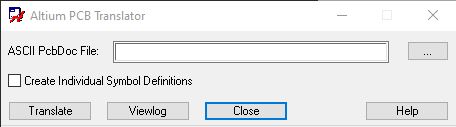
Prerequisites: Project structure
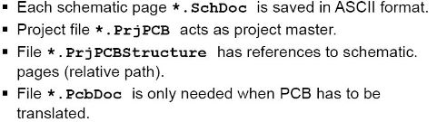
Schematics can be translated only if they are embedded in a
PCB project (.PrjPCB) which manages the design
documents needed to manufacture a PCB design.
Furthermore a valid structure file (.PrjPCBStructure) is
needed. It will be generated after compiling the PCB project
and references the individual schematic pages (*.SchDoc).
If the project file does not exist:
− Select File » New » Project from the menus, the New Project dialog will
open. From the list of available project types, choose PCB Project
− Add the schematic documents *.SchDoc to the project
− Compile the project (e.g. RMB » Compile PCB Project)
− For more documentation about setting up PCB projects refer to Altium
documentation.
Hello,
there does not seem to be an option in Altium to save a library as ASCII (as opposed to a schematic).
I have tried the export function and these are the only files that it generated: Export.zip (69.3 KB)
We also have a Kicad version of the library: https://epc-co.com/epc/documents/KiCad/EPC-KiCad-Library.zip
Let me know if any of these work…
Hello Andrea,
many thanks for the very prompt reply.
Concerning the EPC_2023_Q3a_1.olb, OrCAD Capture managed to open it straight away. The only glitch I have noticed is that pins have lost their pin number.
Not a big deal, as I can easily renumber them in OrCAD Capture anyway.
For the footprints, it appears instead that OrCAD PCB can only translate ALTIUM PcbDoc files (saved as ASCII):
Because the instructions I pasted from the manual in my first message appear to be concerned with the translation of schematic and PCB files, rather than referring to a Library on its own, I am thinking about this other possibility:
starting from a PCB in ALTIUM containing all the parts of the EPC Library ==> save said PCB according to the instructions pasted in my first message
starting from a schematic in ALTIUM containing all the parts of the EPC Library ==> save said schematic according to the instructions pasted in my first message
Would this be relatively easy to do ?
Best Regards
Luca
Thanks Andrea, just tried the translation once more, but I am left with mixed feelings. I report the results here below, in case other OrCADders might be interested:
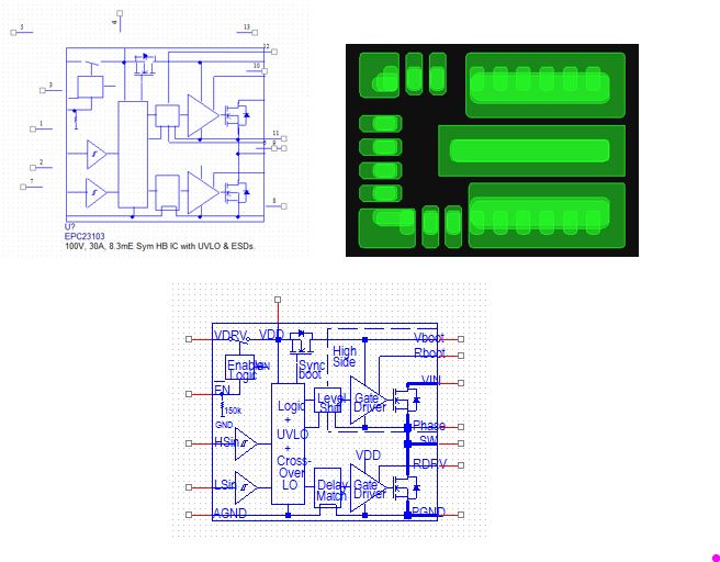
OrCAD Capture appears to successfully translate the schematic (no error flagged). Now the pins are numbered, although placed somewhat at random … in fact the symbol looked better (bottom center) when I had translated the full library epc_2023_q3a_1
Translating then the PCB also produces a result (top right), although all shapes appears to be imported onto the same TOP layer (I am showing only the TOP pins conductor layer, all other layers being instead off), regardless of whether those shapes are meant for resist or paste, etc.
I have just found out about this instructions page from ALTIUM
suggesting the existence of a specific exporter for OrCAD (just for you to check whether it is installed also in your version).
Hello Luca,
I will check out the link you sent, but in the meantime I am wondering if the Kicad library can be of any help: are there any import options for that format?
Hello Andrea, unfortunately OrCAD PCB features import translators only for Mentor’s PADS, PCAD, ALTIUM PCB, Eagle PCB. On this I have also GOOGLEd around, just confirming that such a translator is probably nowhere available.
Just guessing, but perhaps the OrCAD PCB import translator is using that PCBSysColors missing file information in order to import shapes to the correct “layers”. It is perplexing because other layers appear instead to be imported correctly (and indeed those are not flagged with “ERROR”)
the shape for the actual PIN copper land appears to be correctly translated to a PIN SMD onto the TOP copper etch layer
the shapes for its SMD_TOPPASTE and SMD_TOPSOLDER are instead both translated to MECHANICAL PIN, also on the TOP copper etch layer …
In fact, the WARNING covers not only the possibility that the color file is missing but also the case that said file cannot be accessed. Indeed, the warning just preceding it flags that the translator actually found a file named BPCBSysColors but it was unable to open it, suggesting “Check File Name!”
I have searched on GOOGLE for such kind of OrCAD translator errors/warnings, but got no success …
but I would not like to waste more of your time, you have already been very kind, providing prompt support.
So, at the end I can get away with this work around solution:
For schematic symbols: the LIB file you had sent me is fine, as in OrCAD Capture I can then easily renumber the pins of any particular symbol when I will need it.
For PCB symbols (with footprint): I will just import it ==> keep the actual electrical PINs, while deleting all the mechanical PINs (which corresponds to erroneously imported SOLDER and PASTE shapes) ==> finally redrawing all SOLDER shapes directly in OrCAD PCB (into the class/subclass named Package Geometry/Soldermask_Top) as well as the PASTE shapes (into the class/subclass named Package Geometry/Pastemask_Top). As I draw them on top of the underlying electrical PIN shapes, the overall process takes no more than about 20 minutes (now that I know how to get around it …).
Hi Luca,
glad you can at least move forward.
By the way, the exporter you mentioned was already installed, it’s what enabled the first export files I generated…
Good luck!