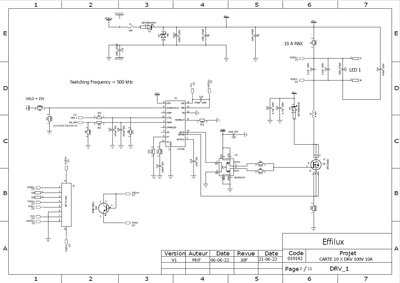
I’ve used an EPC2010C GaN FET as a switching device in one design for driving LED :
- 10 LED Drivers / board
- IMS PCB 2 Layers
- Total Power : 6 kW
- 80V input
- 60V LED String Voltage
- 10A / driver
- The PCB is screwed on a metal plate with water cooling (water at 20°C).
Problem :
Before powering up, the Drain-Source resistance is higher than 10 MegOhms (leakage current very low). After working for one day, the Drain-Source resistance on all GaN transistors is about 600 Ohms (leakage current of 20 mA).
It’s the first time I use GaN transistor. Is there any case where the leakage current can increase ?
Hi Fontamax,
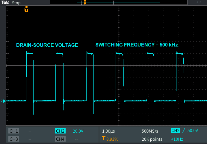
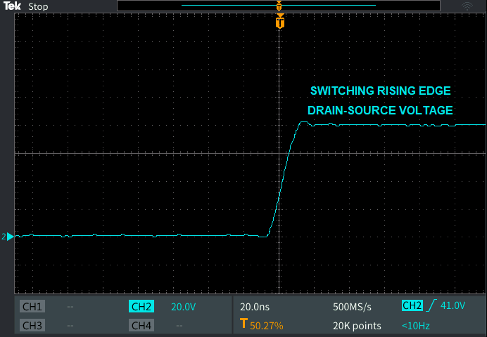
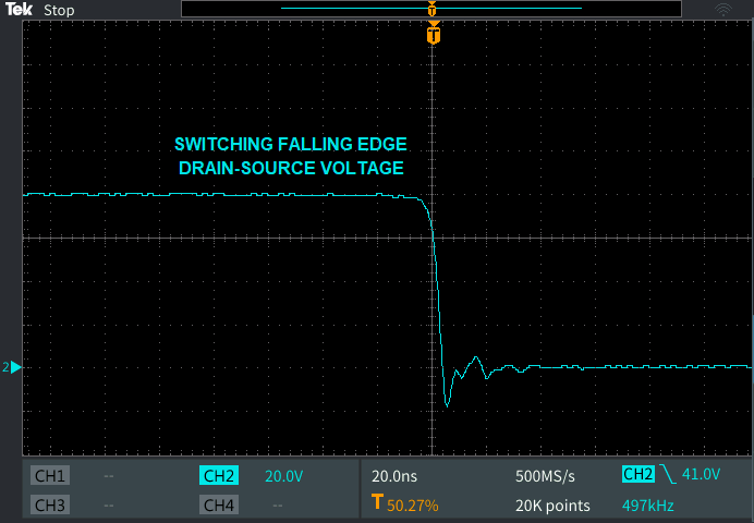
I would say this sort of degradation is not normal. What topology are you using? Do you have a switching waveform of the drain to source voltage (zoomed in during the switching transient). I’d like to make sure you are not exceeding the rated voltage.
By the way, for new designs we recommend the newer EPC2207: 200 V, 54 A (epc-co.com)
Hello,
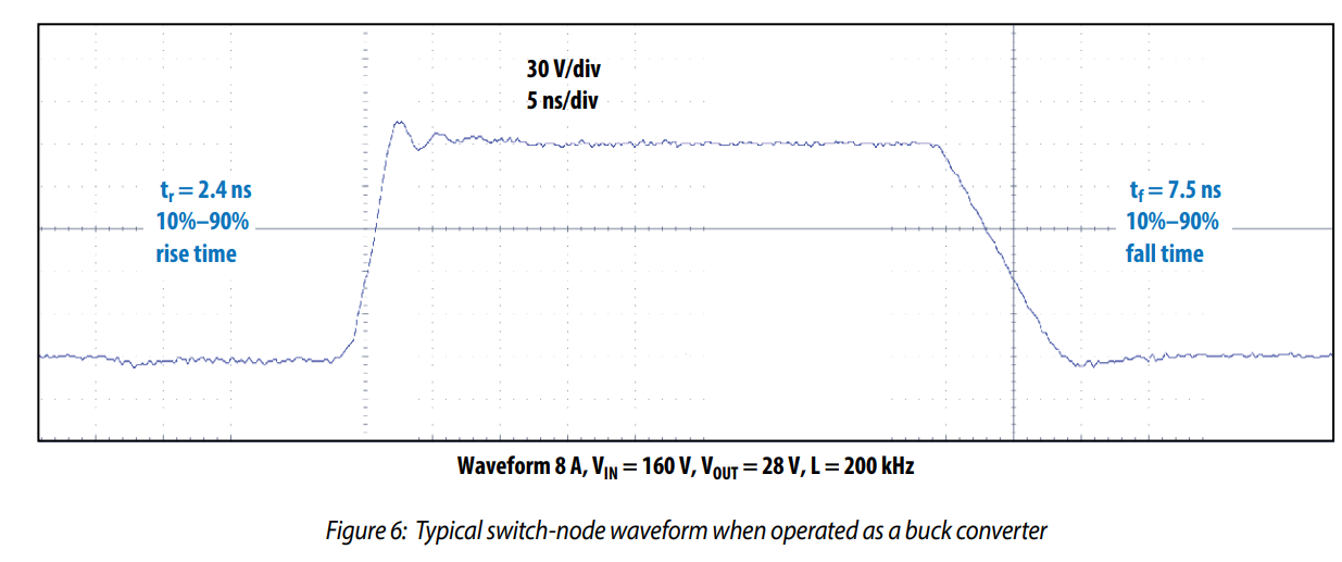
I am wondering how close to the FETs you are doing these measurements, and the bandwidth of the scope and probes? We have some recommendations here: AN023 Accurately Measuring High Speed GaN Transistors.pdf (epc-co.com)
The undershoot seems quite large, hence I am wondering how close you the device you are measuring.
The rise and fall times also seem very slow, especially since you are using 0Ω gate resitors
To give you an idea of what to expect you can look at the half bridge board for EPC2010c: EPC9003C_qsg.pdf (epc-co.com)
I also would like to say that the shunt resistor in series with the Source is a critical part of your design: it is very important to minimize the stray inductance impact of it.