Dear EPC forum,
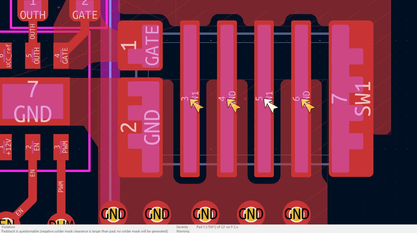
I am currently finishing a PCB layout of a 500W SMPS. The last remaining design rule warning is caused by the EPC2304, stating: “Padstack is questionable (negative solder mask clearance is larger than pad; no solder mask will be generated)”.
In all honesty I do not have any idea what this implies, or if it is even a true error. If you know, please let me know what is going on, and how I might solve this issue. Thank you.
Hello,
we have used in the past Kicad successfully. The reason why the “clearance is negative” is that our landing pad is solder mask defined, so pad solder mask opening is smaller than pad copper. This is fine.
I suggest to:
- generate the gerbers
- verify on the gerbers if the solder mask is correctly generated (as expected in the EPC2304 datasheet drawings).
- if you see issues in the solder mask, or the solder mask has not been generated as the message says, please check for options to ignore the above error.
Regards