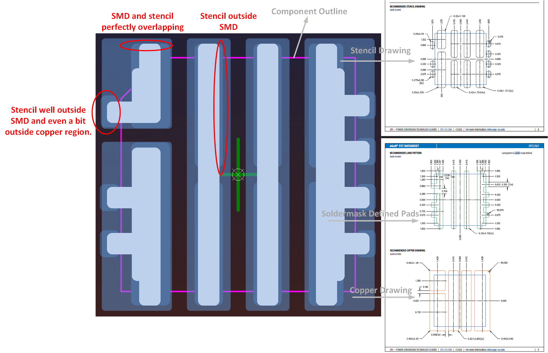
I’ve designed the EPC2367 footprint according to the datasheet (as shown in the image). I’ve circled a few places that look odd to me, like the stencil being larger than the soldermask defined pad (SMD) and sometimes even sitting outside the copper are, but wanted to confirm it is indeed intentional. If a PCB assembly house sees this footprint, will they tend to pull the stencil back within the SMD area? Seems like a note is needed in the PCB assembly drawing to ensure they don’t do that.