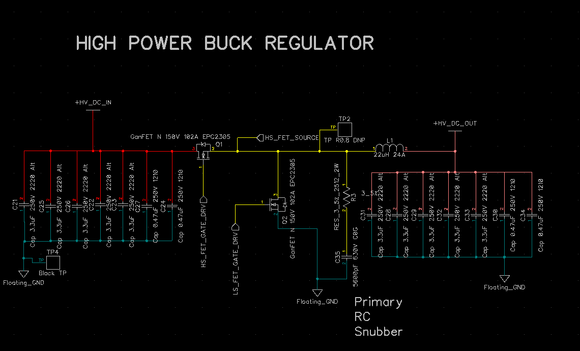
We are working on a DC-DC Synchronous Buck type application with Input voltage being around 65-70V and output duty cycle being 0% to 100%. For this we utilize a SW_NODE referenced floating supply. Output current we need is about 17-18A however we can only run about 12-13A before the Gan driver fails.
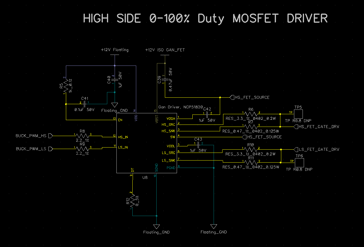
And below is the schematic for the Gan driver which uses the NCP51820 which is also the driver recommended in the EPC90143 eval board for the EPC2305 fet.
At lower current values everything works as expected and up to around 12A of output current all works as expected with both driver and HS fet at around 60 degrees C when using a thermal camera. However when going beyond that we have a failure of the gan driver NCP51820 where the LS_SRC and LS_SNK have <5Ohm connection to VDDL and in that condition gate driver ends up drawing >100mA causing it to heat up to around 110C before we realized the failure. This has happen on 3 separate drivers now causing us to believe there is something wrong with the design on our end.
Any opinions on this would be helpful as this gate driver is used for the Eval board by EPC.
Hello there. In general terms, issues at higher currents implies issues at higher di/dt, or higher induced voltages on parasitic inductances on your loops. If the common source inductance is not under control, that could explain your issues.
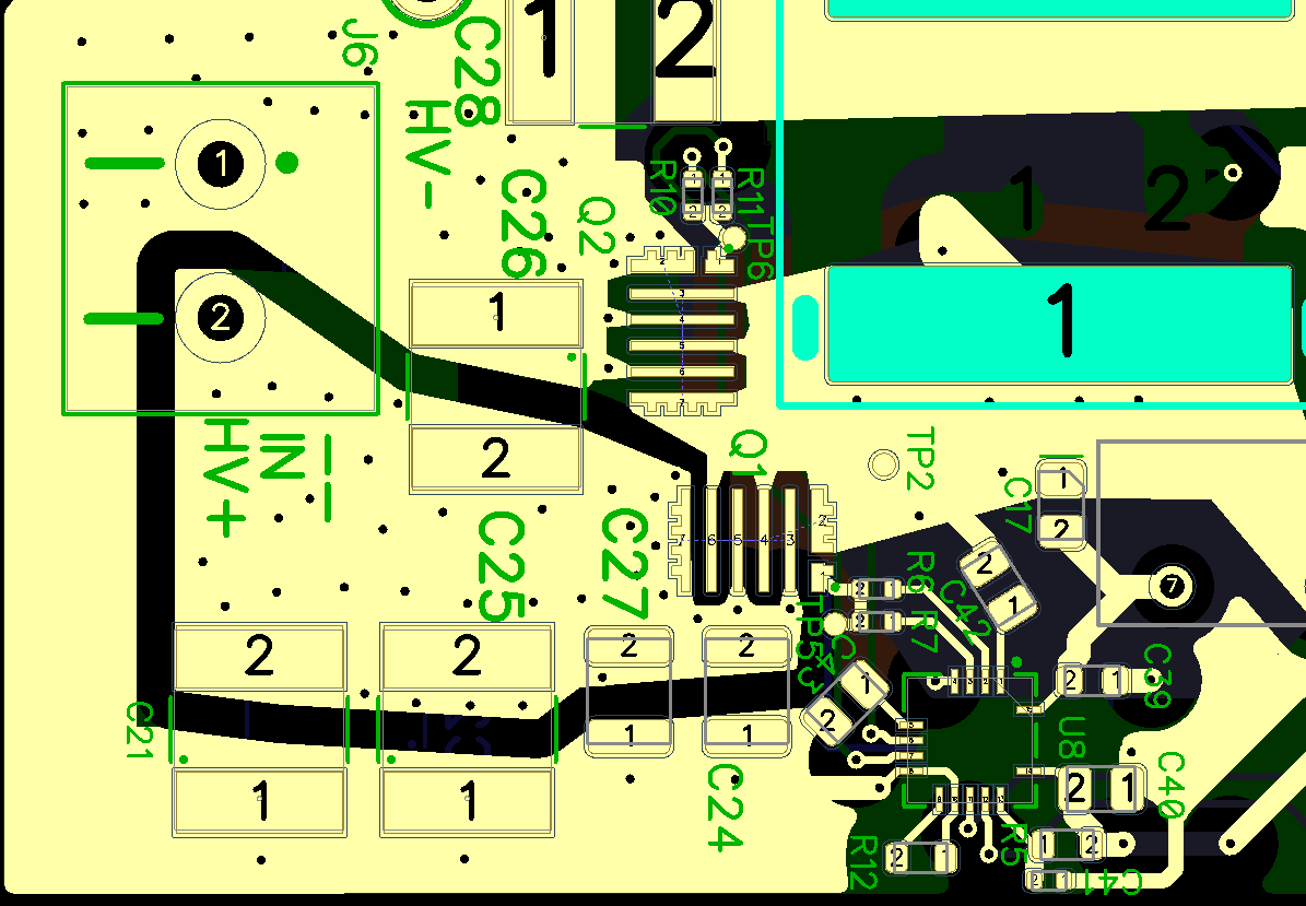
Make sure your layout resembles that of the evaluation board to rule-out layout induced issues.
Also, I don’t see the bootstrap diode with accompanying limiting resistor, refer to the driver’s datasheet.
Due to limited component placement abilities a tradeoff was made to route the HS fet in an optimal way while routing the LS fet in a more suboptimal way due to the driver vs fet placement.
Internally we also concluded that it was dI/dt related but it wasnt as clear about what the solution should be. We will probably end up trying two of the 1EDB7275F drivers that is listed in the main drivers so we can optimize each fet loop independently.
As far as the bootstrap diode and resistor, we are running the HS fet in a 100% duty cycle configuration where its on for extended periods of time. Due to this we have an Isolated 12V(Floating_GND referenced) to 12V(HS_FET_SOURCE referenced) DC-DC converter to provide the HS gate drive charge for 100% duty operation. This circuit works fine and we have verified that in this mode of operation we can run the HS fet on continuously.
Thanks for the common source inductance hint, thats very likely the problem for the LS fet gate loop.