I am looking at the documentation for the EPC9172 development board and checking the EPC21701 laser driver design reference.
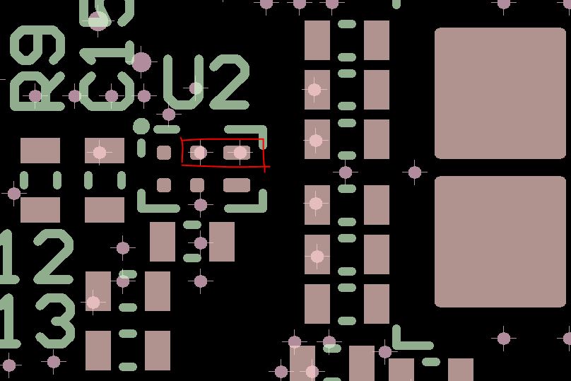
Looking at the EPC9172 PCB Gerber file, I noticed that the EPC21701 pad has a via hole added to it.
I remembered someone’s advice not to add via holes to pads due to poor SMT.
Is it OK to add via holes to the EPC21701 pad?
What is the diameter of the via hole?
Can I get the EPC9172 Altium file so I can study it more closely?
Thank you.
Hello,
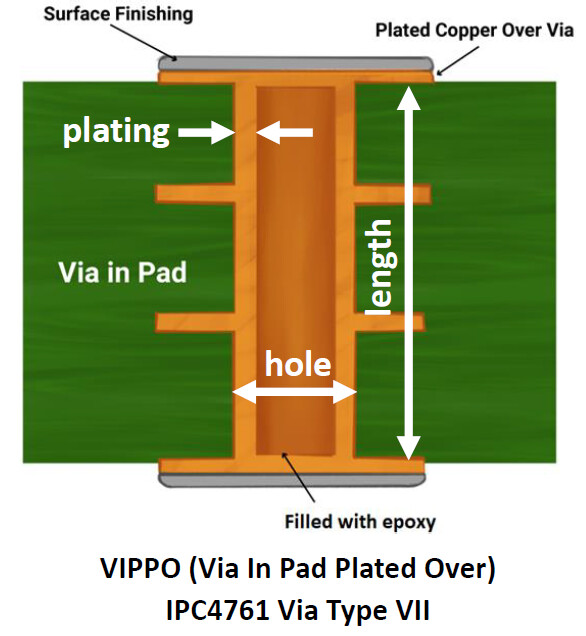
we are suggesting to use vias in pad plated over to minimize the thermal and electrical parasitics. This means the hole is filled with epoxy, and then plated over.
This way there is no risk of solder wicking during assembly.
In most cases we use 0.2mm drill on 0.35mm diameter via pad.
Hope this clears your doubts.
To get the Altium files you need to contact your local FAE, see here:
https://epc-co.com/epc/about-epc/contact
Best regards
Hello, Thanks for your inquiry.
I’m local FAE for Korea and I had emailed to you to support your inquiry, so pls check my email.
Thank you again.