I have read the datasheet as well as several other sources on the EPC2121 transistor and I am wondering how it is structured internally. I suspect that it is a back-to-back structure consisting of two unidirectional GaN HEMTs (B2B-2UDS). Various aspects of the datasheet seem to indicate this. However, it is not explicitly stated anywhere whether the EPC2121 is indeed a B2B-2UDS transistor or whether it is instead a monolithic bidirectional switch.
Could you please confirm whether the EPC2121 internally consists of a back-to-back structure with two unidirectional GaN transistors? How can this be identified unambiguously for the EPC2121 based on the information currently provided in the datasheet?
Sorry if my question sounds a bit naive; I am still relatively new to GaN technology.
I am also wondering this. Do you by now have more information on this topic?
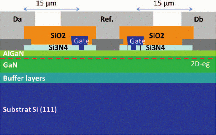
In this paper, the authors describe a monolithic device with a single reference (with which I believe they mean source). See also the figure from that same paper:
I believe the EPC2121 to have (more or less) the same topology. (This is a guess, I do not work at EPC) However, looking at the simulation files given on the product page, for example the LTspice .lib file, a behavioural current source is present that models a current directly from drain to drain (lines 33-37, bswitch1 drain1i drain2i I= ... ). This is on top of two other current sources that simulate the drain-source currents for both drain.
Now the question that I have after these observations/guesses on topology: what is the physical background of this current source in the model. Since the 2D-electron-gas layer always crosses the source region, how can there be a current through a gate-source region if the gate-source voltage is zero. (Which happens in simulation if source has a lower potential than both drains.) What happens there? Is there an energy band diagram that can shine more light on this? Is this real behaviour, or just the effect of a parameter-fitted model?