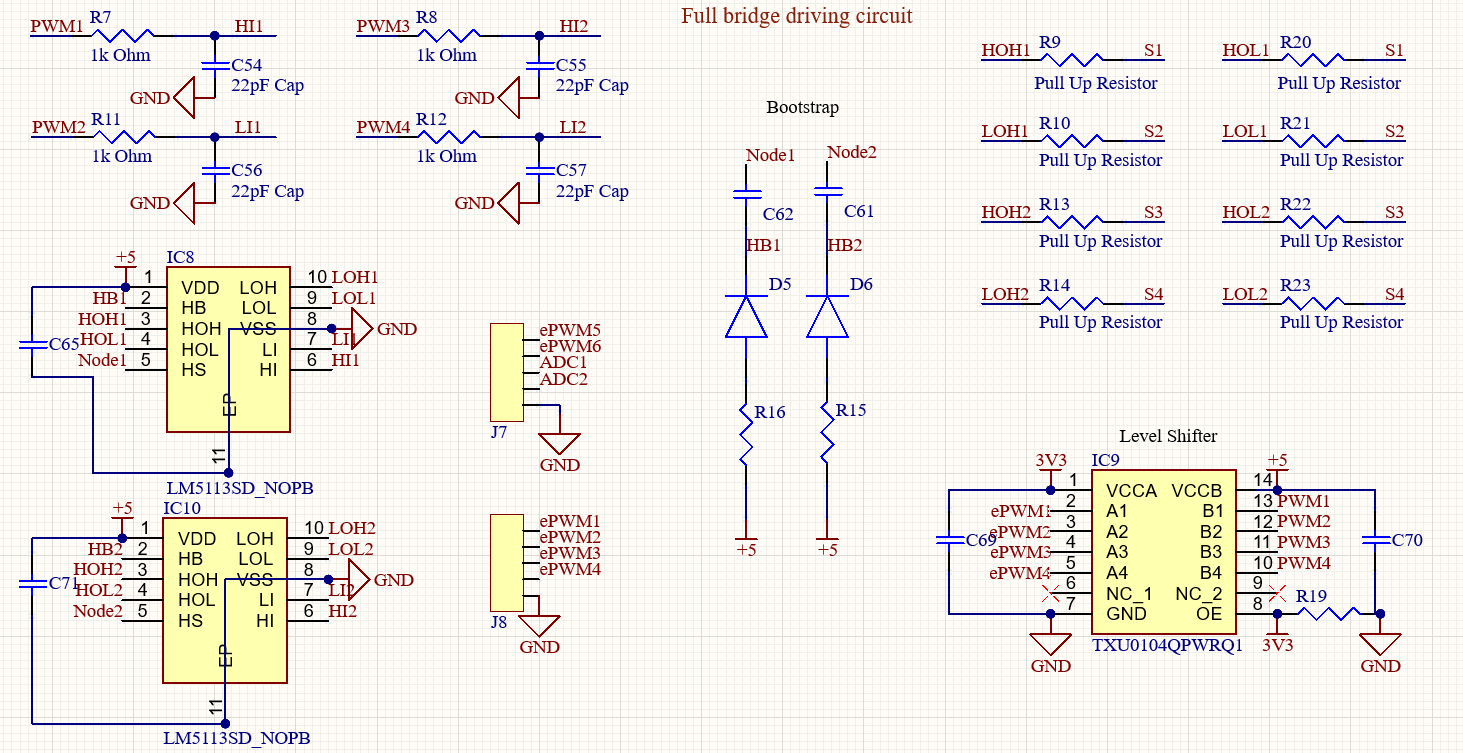
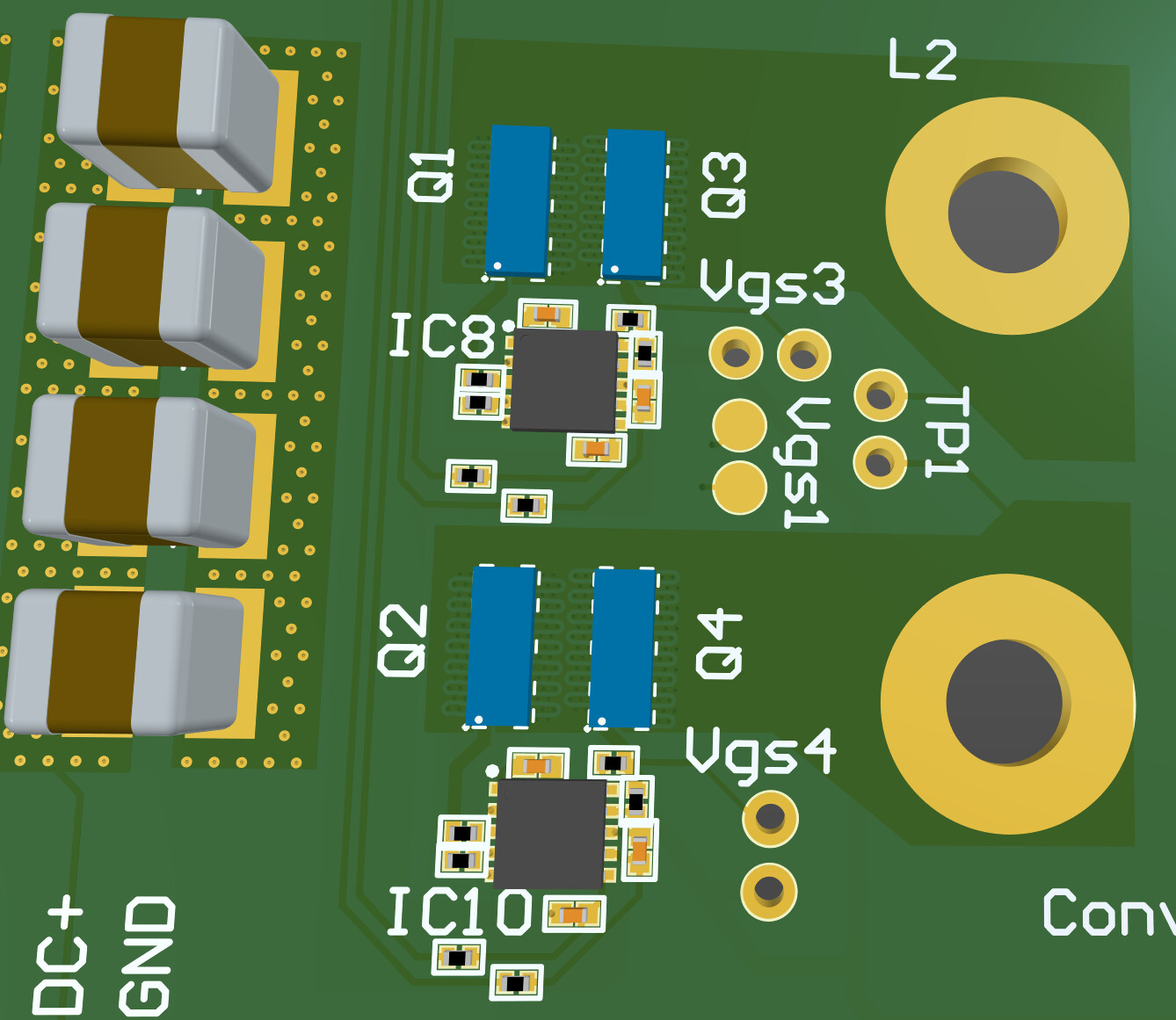
I have created a PCB of the circuit in the schematic below, with the full bridge consisting of EPC2021 devices. The driver is TI LM5113, with a 4.7 ohm turn-on and no turn off resistors in place.
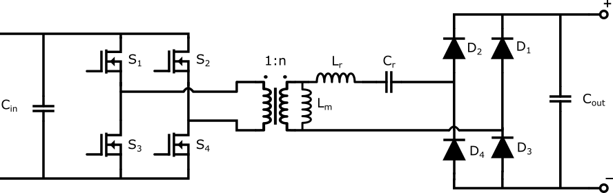
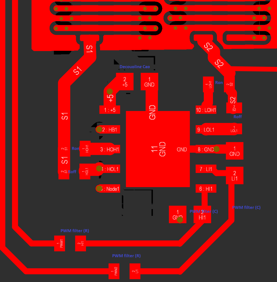
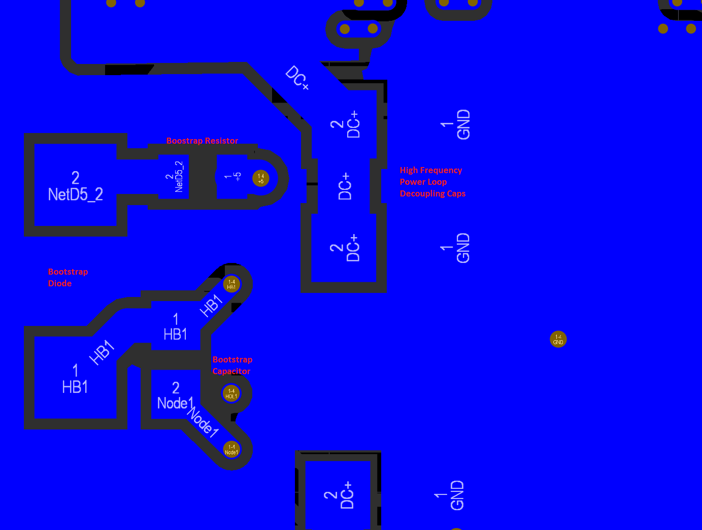
Unfortunately, as the input current is increased, I see some ground jumps in the gate signals, followed by a high-frequency oscillation (~120MHz). I’m trying to figure out what is the cause of this problem, so far I’m thinking it looks like a common source inductance problem on the gate drive and power loop (?), as also changing the turn-on gate resistors doesn’t seem to have much effect. However, I’ve designed the board so that the gate and power loop currents flow at 90 degree angle (so hopefully zero mutual coupling), and also have source vias to return the current to the gate almost on the device’s source pad. I’m attaching the problematic waveforms, if someone has encountered waveforms like this, I’d be very grateful for some insights.
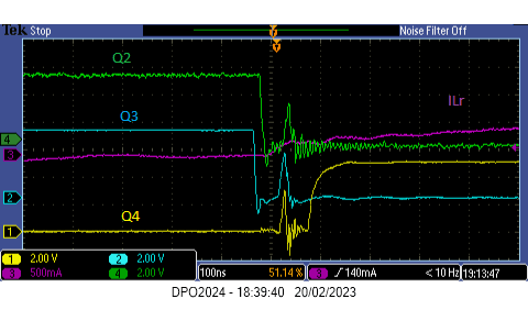
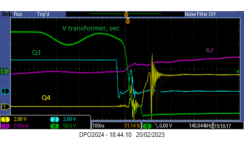
However, this phenomenon doesn’t seem to appear on the opposite transition (low->high) of the transformer.
Hello Greg.
I have a couple of hypothesis to be checked.
The first one is that the transformer is DC coupled at the driving side, and this could cause the flux walking on one direction because of the DC component that might be there because of some asymmetry in driving. The core then saturates. This could cause the issue in one transition but not in the other. Also the Vtransformer shows an hesitation in the lower part of the falling transition, which is not there in the rising. You should try to AC couple the transformer at primary and see what happens. And also add a small gap, but not sure here since I miss the details of the transformer.
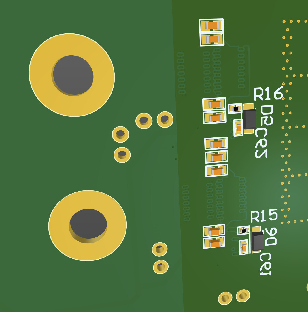
The second is that something happens in the driving of the GaN FETs. We would need the schematic and layout to double check if we can find some reason for this problem. Also, usually we don’t recommend 0 Ohm turn off resistor. You can check what happens if you place 1 Ohm or so Roff.
In general, for a new design, we recommend to replace the Gen4 EPC2021 with a Gen5 EPC2071. The EPC2071 can be mounted in the same PCB, and has a better structure of the Cgd / Cgs that should be more robust against RF oscillation. It also has a 20% lower Coss.
Thank you a lot for your reply; I’ve been troubleshooting this issue for a while now and I believe the problem was with improper grounding (transformer dv/dt creating ground jumps), and incorrect placement of my PWM filter (RC circuit was positioned quite far from the actual gate driver).
I’m going to be trying again with a new board. Should you have some time, I’d be very grateful if you could take a look and tell me if something on the layout seems off.
Please have a look to the “optimal layout” described in this appnote.
It seems you used a vertical layout, which is not the best in terms of power loop inductance. Also not clear where the bypass capacitors are placed, they look to be on a side, so I see some room for improvement. Then, is it a 2 layer PCB? A 4 layer PCB would reduce the parasitics significantly.