I followed EPC2302 datasheet to create the footprint in my design, and it was not too different from the footprint on the EPC_2024_Q2a.IntLib that I just downloaded today.
Is it something to do with the automatic assembly process than a hardware design error?
I read from the EPC assembly document that you recommend using ENIG 3U" to 5U" thickness,
but my PCB was manufactured with 1U" ENIG.
Will this be a problem?
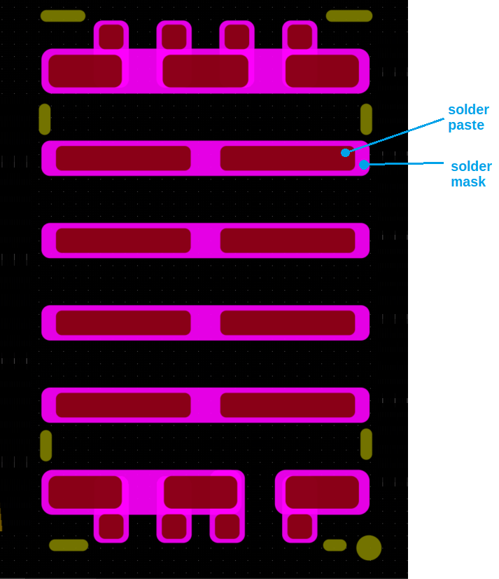
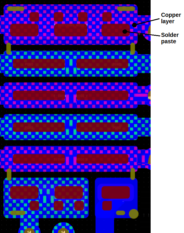
Yes, the solder paste stencil design may look a bit odd, but it is correct. It is designed for best solder coverage not only under the FET, but the sides of the device pads. I noticed that some other QFN packaged devices from some other manufacturers use a similar solder paste stencil design (not an EPC-only recommendation).
ENIG: the recommendation is to follow the standard, IPC-4552, which covers all boards (not just for EPC devices), it lists 3-5 u". We don’t have experience trying various Au thicknesses… this seems to be a general assembly question, not specific to EPC devices.