Hi, Sir.
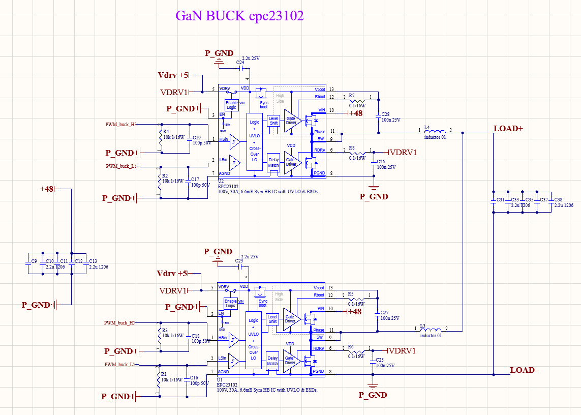
I want to use the GaN IC EPC23102 to design a two phase interleaved buck converter, and I designed a pcb with reference to the schematic of EPC9177 and datasheets. But my pcb board can not work. I don’t know why it was happened. The following image is my PCB schematic diagram. Could you please help me check if there are any issues with my circuit design?
**a) The net "Vdrv+5 " is the power supply of ICs. And I directly use a DC power supply to supply 5 V without using a power IC. **
b)I do not sure if the “EN” pin can be directly grounded. I found out in the datasheet that the “EN” pin is grounded, so I also grounded it here.
Hope to your reply.
Thank you so much.
PWM voltage is 3.3V
PWM voltage is 3.3V
PWM voltage is 3.3V
PWM voltage is 3.3V
dsp: tms28379d
Dear Kristen,
This is Richard Zhu from EPC China. My work location is in Shenzhen and my contact information is +86 18680665001(richard.zhu@epc-co.com) and if you have further questions, please contact me directly to give you on time support.
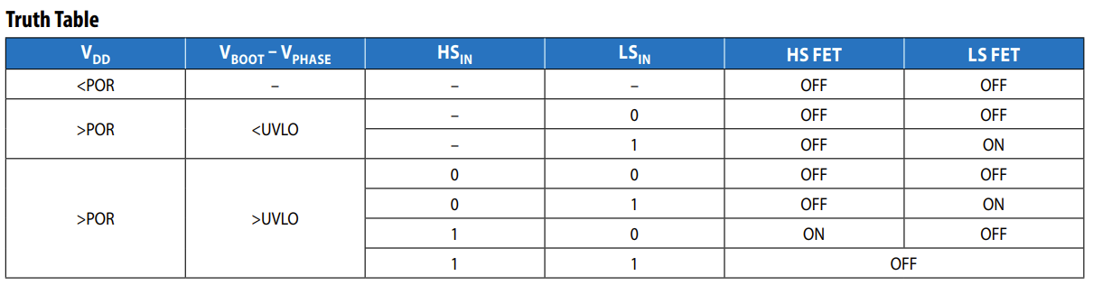
Regarding your question, the truth table of EPC23102 is as below:
,
- Did you check Vdd is greater than Vdd_por?
- Did you check Vboot-Vphase?
EN pin is used to bypass the power supply in case the IC is not switching to minimize the quiescent current. If it is grounded, this function is disabled.
What is your switching frequency? C25,C26 should be changed to 2.2uF and place them as close as possible to the pin of EPC23102.
My switching frequency is 200 kHz.
Must C25 and C26 be 2.2uF? Is it 1uF OK?
1uF should be OK. Check the ripple voltage during switching.
What is your contact information like e-mail address?
I want to check with you how to calculate the Cboot based on your switching frequency and duty cycle. and also the PCB layout design is critical and we hope to go through it with you.
My email address is 1550032361@qq.com.