Hi,
Could anybody shed some light on this failure mode?
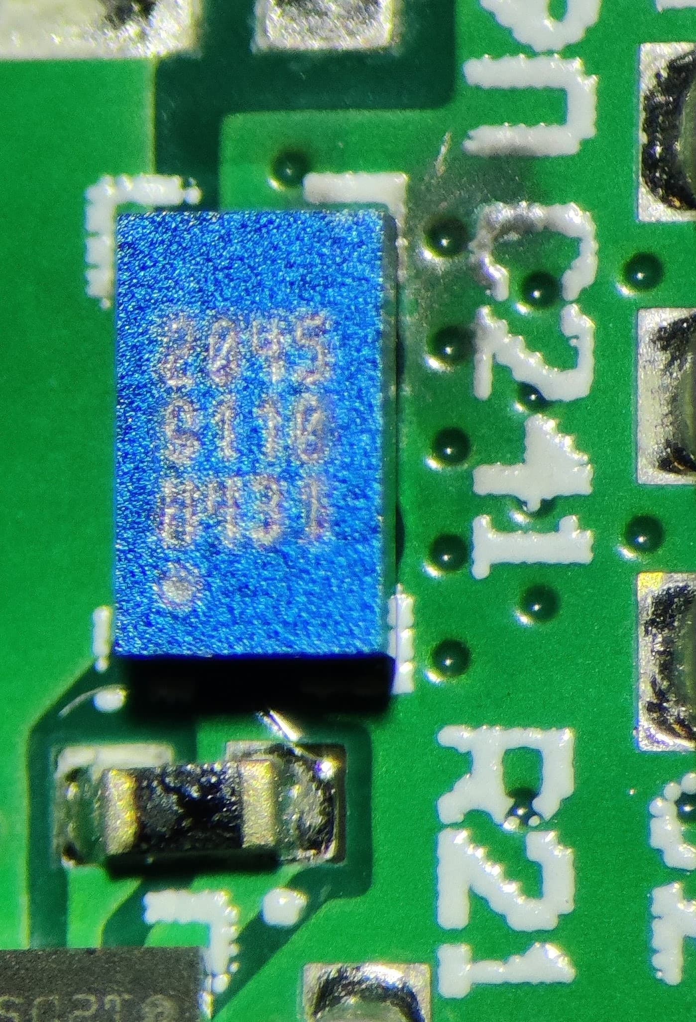
The two GaN FETs (EPC2045) in the pictures was used in a motor drive application in a half bridge configuration at 48V@80kHz and believed to be working at around 7A peak current in less than a few milliseconds.
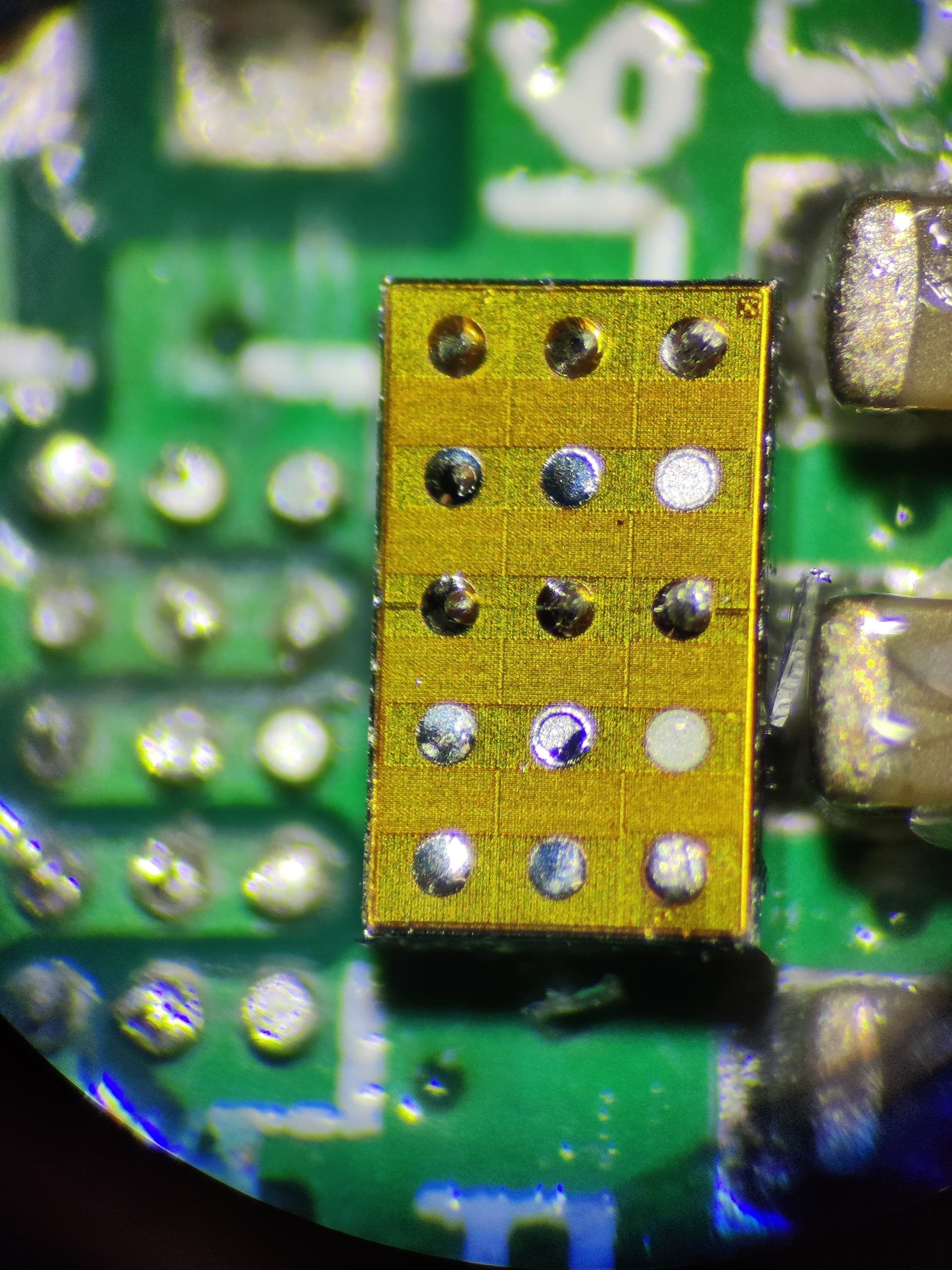
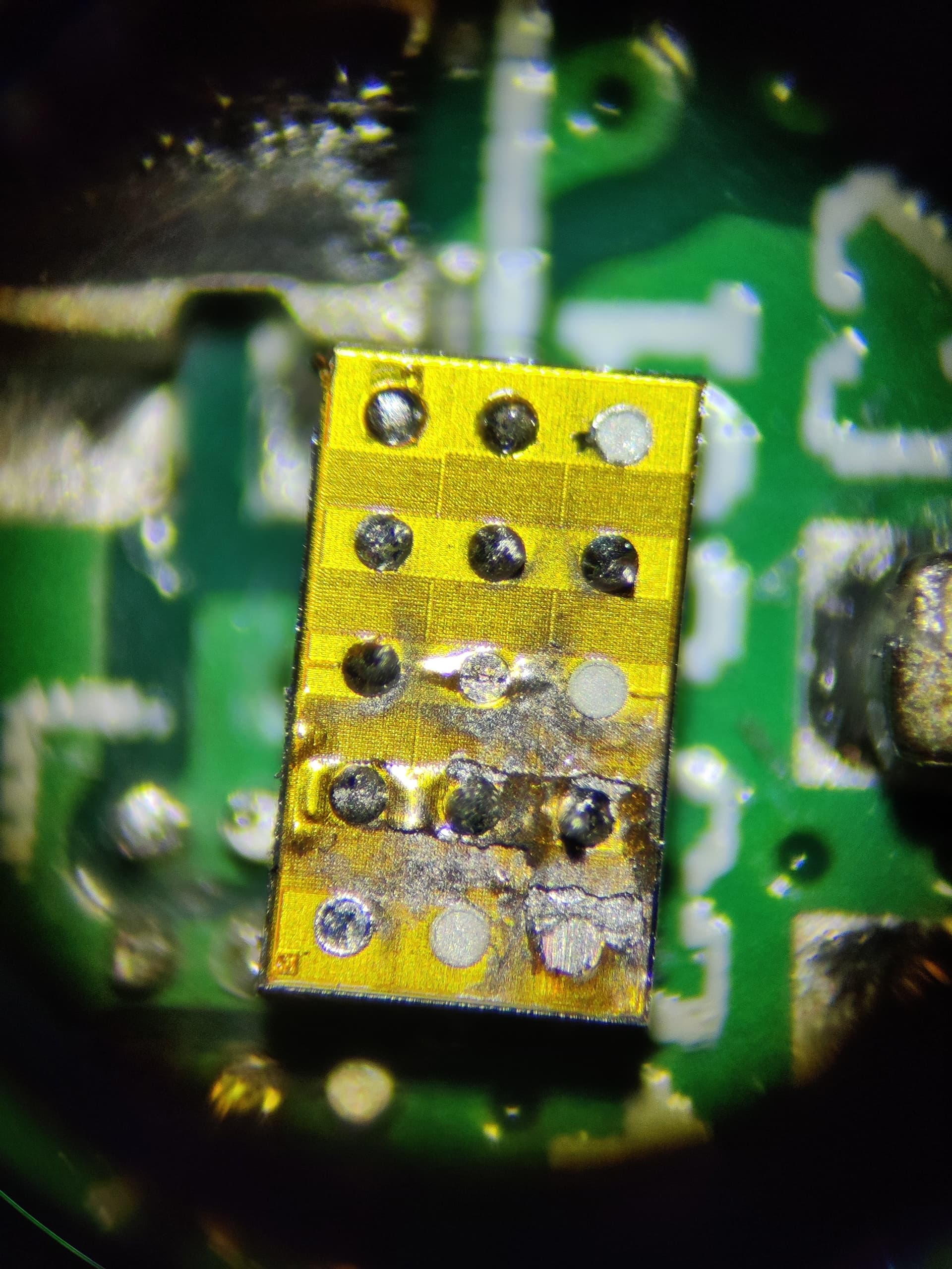
The low side FET failed, shorted to gnd and released the magic grey smoke which turned into a sticky gooey on the board. Looking at the device in a microscope it looks like it cracked and burst on the underside which is consistent with the direction of the ejected gooey on the PCB.
Does anybody have some insights here?
Hello.
That kind of failure looks an electrical over stress (EOS) causing a burnout of the active layer and melting/vapourizing the metal layers.
It is the result of excessive power dissipation. It is usually related to an overcurrent, leading to I^2 * Rdson losses that cannot be thermally handled. It might also be caused by driving the GaN FET into its linear operation region, with Vgs slightly above its threshold value, and simultaneous current flow + Vds drop. Finally, it might be caused by too high frequency switching, leading to excessive losses.
So please check carefully the working conditions that caused the failure, against any overcurrent, bad gate drive, or unexpected high frequency switching / oscillation.
Regards