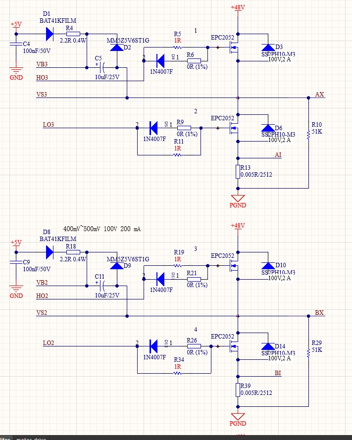
Hi! I have been designing motor drive circuit with EPC2052.Here is my schemaitc.
Can any please help me?Am I using the EPC chips right?Thank you so much!
Hello,
of course!
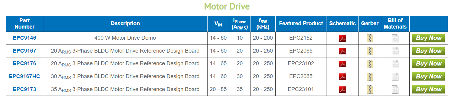
As a starting point have you seen our reference designs for motor drives? EPC Evaluation Kits for GaN Devices (epc-co.com)
They can provide good guidance on schematic and layout.
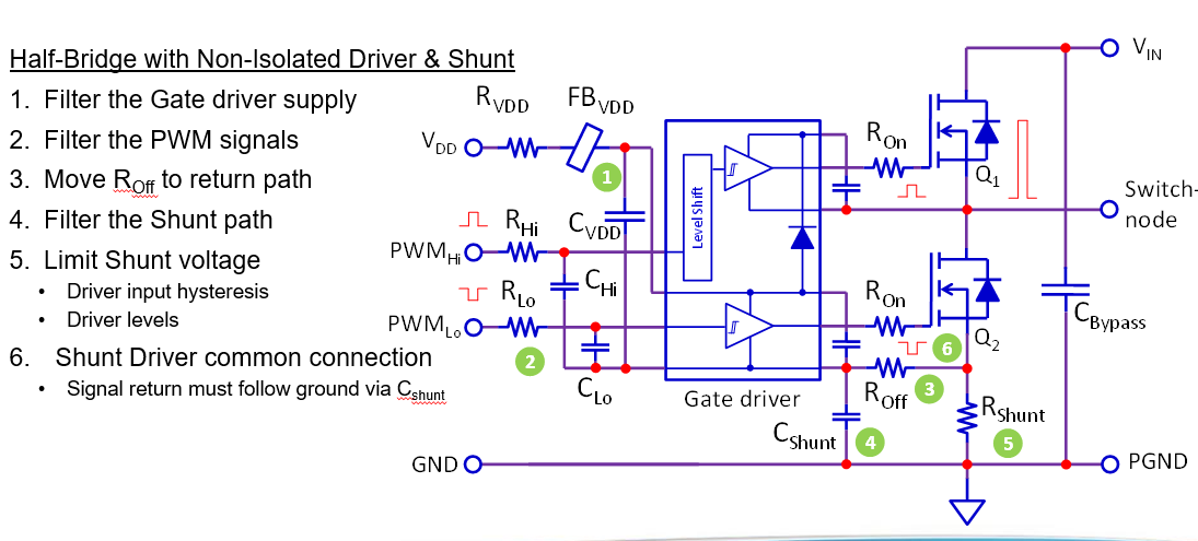
For example in your schematic you are using a diode to speed up the turn OFF. However we recommend against doing so because Gan FETs threshold is fairly low and the diode voltage drop will interfere with the turn OFF.
If your gate driver does not have separate pins for ON and OFF, go ahead and use a single gate resistor.
Also for the low side shunt you need to be careful how to handle the Source of the low side FET vs PGround.
If the gate driver you selected has separate logic and power ground:
- the gate driver return should be referenced to the Source to provide minimum common source inductance and a strong turn OFF
- the gate driver should be able to withstand the shunt voltage drop (with ringing) between the logic ground and source reference
if the gate driver you are using does not, you can try this approach:
Thank you so much!
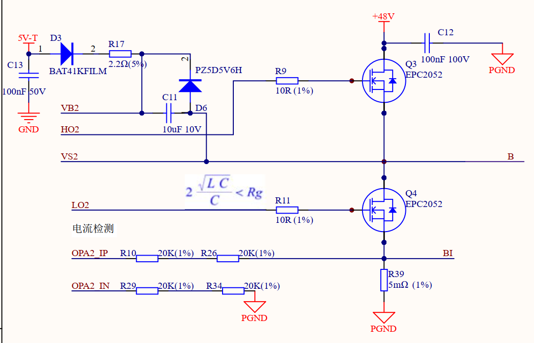
I changed the schematic according your opoion(The picture is the new schematic).Maybe I did it wrong,the PCB come back and it doesn’t work well:
I try to output PWM to the GaN,The GaN has no output.So I turn off output and It seems one of the GaN is broken.The voltage of VS2(B) is 44V(even if i remove the R9).So I think the GaN is broken.Do I design the circuit wrong?How can I fix it.
Sorry If I didn‘t describe my problem well.
Hello,
I’m sorry to hear about your issues.
To review the schematic I would need to see the gate driver also, and probably the layout. However, from the description of the problem it seems far more likely that it is a manufacturing or assembly related issue since the parts might have arrived broken already.
The first thing to check is that you have followed our footprint recommendations including using solder mask defined pads. This is described in the datasheet and in more detail in How2AppNote008 - Designing PCB Footprint eGaN FETs ICs.pdf (epc-co.com). We also provide an Altium library with all our footprints: this is the easiest way to implement this topic. Also be sure to double check that the PCB house did not change any of the gerbers, as it sometimes happens with these fine pitch components and it can create issues.
Finally the PCB and assembly house should be careful when handling these components, especially if any manual handling is involved (including rework). We have some guidelines on assembly here: Appnote_GaNassembly.pdf (epc-co.com). If you suspect any mechanical damage you can use this document GaN_Visual_Guide.pdf (epc-co.com) to guide you.
Finally, since I think you are located in China, it might make sense for you to talk to our local FAE there. Can you tell me in which region/city your are located?
Hi!
I’m sorry for not replying for so long.
It’s the gate driver MCU’s problem.The MCU I chose didn’t support 5V.So I changed MCU and now the outputs of the GaN are right.
In the mean-time,I have been reached out bt the FAE.
Thank you so much!
that’s great! thanks for letting us now the root cause, and good luck with your project…