Dear EPC,
I am designing a LIDAR transmitter (low power) using your EPC2212 GaN FET and reference design that you have on the web page. You recommend connecting source and substrate on the GaN FET. I read on TIs web page, on the other hand, that they recommend in their LIDAR transmitter design (also using EPC GaN FET) “the power loop ground and the gate loop grounds are separated and tied together at the single tie point inside the FET. This combination ensures that no current from the power loop flows through the gate loop and causing a ground lift.” So they have separate power ground and gate ground. Which one to implement??
Hello,
please note that TI reference design TIDA-01573 used EPC2019, which is an old part with separate substrate pin.
Also this is not the best reference for the layout.
The sentence should be rephrased to:
“The power loop ground and the gate loop grounds are separated and tied together at the single tie point inside the FET next to gate pad of the FET. This combination ensures that no current from the power loop flows through the gate loop and causing a ground lift.”
Then the substrate pad needs to be connected to the same copper on the PCB as the other source terminals. Please consider for your application the newer parts EPC2051 or EPC2204 / EPC2204A, for which the substrate is connected internally.
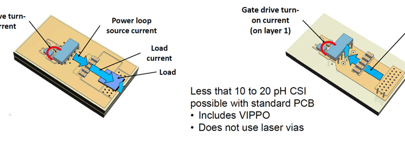
Please see below a suggested layout, that can be implemented on a 4 layer PCB. The Laser driver is implemented in the top 2 layers.
As you can see, gate loop is layout on layer 1 (top). Layer 2 is providing ground plane for gate driver.
Power loop is layout on the opposite side of the GaN FET, in order to minimize CSI.
It is important to use the minimum allowed insulator thickness between L1 (top) and L2 (inner). Usually it is 2 to 3 mils.
Regards