EPC2218 is used for full bridge inverter, with 28V and 20A loading.
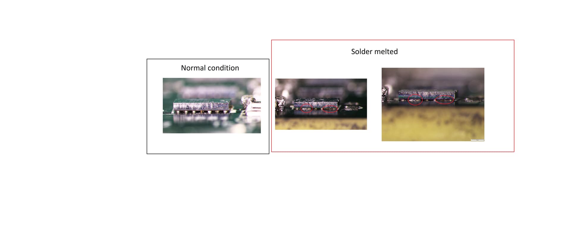
Referring to the picture above, I’ve observed that some of the GaN FET solder bump looks weird after a few test, anyone encountered similar problem? Please advise on the possible causes of the phenomenon, thank you.
Hello,
GaN FETs tend to be very robust. It has happened before that the solder will melt while the device is still OK. This means that the temperatures have exceeded the melting temperature of the solder.
What is your expected operating temperature during the tests you are performing?
Could you please monitor the temperatures of the FETs (IR camera, or thermocouples)?
The electrical/thermal over-stress condition should be addressed so that the operating temperatures stay below the max Tj allowed on the datasheet (150°C).
Hi Andrea,
For my application, I have observed roughly 90 degrees on the GaN FETs using IR camera. (10 seconds of testing)
After placing a heat sink on top of the GaN FETs, I monitor the temperature using thermocouples placed right beside the GaN FETs, touching the PCB only, which is around 50 degrees. (60 seconds of testing).
With the above results, the expected operating temperature during test is below 100 degrees at GaN junction, therefore I could not explain why the solder melted.
yes, those temps are within Tjmax, however they do not explain the melted solder (200°C?). Maybe there was a transient that you did not capture in the temperature measurement?
Sorry for the late response, yes there is a possibility that there is a transient raise in temperature, but that would be something that we cannot capture.
I was wondering if the underfill would hold the solder in place when melting occur?
Also, referring to the photo in the original post, could it be dendrites?
The underfill should be able to hold the solder in place. However, the Tg of the underfill material is significantly lower than the melting point of SAC305, so this might lead to unexpected behaviors.
In the picture we can mainly see melted solder.