I’m currently designing a PCB for my use with EPC GaNs on which I want to use the synchronous Bootstrap from the EPC 90133 Demo Board.
Can somebody help me to understand the function of the Diode D77? Because this Diode isn’t mentioned in other publications and I don’t see the point of having it.
Thanks a lot.
Hello,
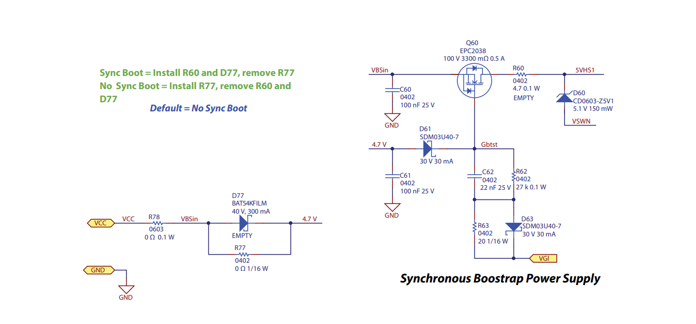
D77 works in conjunction with the rest of the circuit. These are the main functions of this circuit:
- D77 charges C61 (Vdd of gate driver) to 4.7V to keep the gate driver internal bootstrap diode from conducting
○ Internal bootstrap diode has 5V on cathode (Cboot) and 4.7V on anode (Vdd). It is reverse biased and cannot conduct. - D61 (and D63) charges C62 charging to 4.0V
○ When LS Gate is 0V (OFF), Gbst is at 4.0V and Sbst is at 5V. BootFET is reverse biased so it’s Vf is higher than the main LS FET and always presents a higher impedance path than the main LS power path - R63 is in the BootFET gate turn ON path and introduces a small delay in turn ON
- D63 is in the BootFET gate turn OFF path and is for fast turn OFF
That makes absolutely sense, I didn’t thought of the internal Bootstrap diode. Thanks a lot for your quick reply! Have a nice evening