Hi,
I’m designing a DCDC converter using a half brigde GaN Fet (EPC2103). I’m not sure how to use HS Return pin of the device. According to data sheet, the pin #3 is high side gate return and connected internally to the switching node. Does it mean, this pin should not be connected to the switching node externally?
Thanks in advance for your support.
Hello,
you are correct, this pin is used for connection to the driver, the connection to the switch node is done internally. You can also take a look at EPC9039 (epc-co.com) for a layout example.
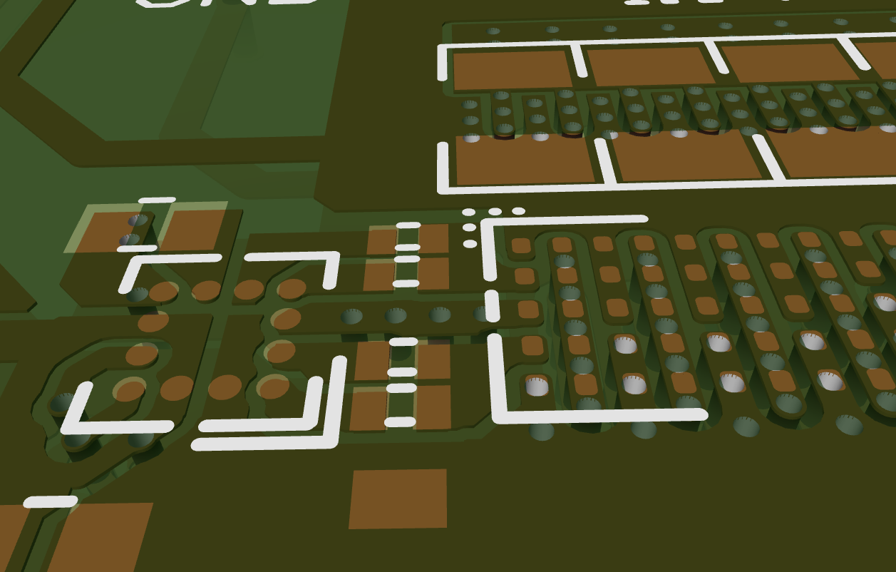
I tried to capture a snapshot of the area of interest:
You can see pin 3 connected to the gate driver HS pin.
I hope this helps!
Thanks for your reply.
I see 3 vias between GaN device and gate driver HS pin, after investigating the EPC9039 gerber files, I realised that this 3 vias are used for the bootstrap cap connection. So the eval board does not connect HS return pin with the switching node externaly.
Regards,
Özgür